Subscribe to Updates

    Get the latest creative news from FooBar about art, design and business.

    What's Hot

    Tide turning in Europe’s smartphone market despite 6% shipment decline in Q3

    November 29, 2023

    Blaupunkt Redefines Sound Excellence with BE100 XTREME Neckband

    November 28, 2023

    Sony India unveils INZONE H5 wireless gaming headset to elevate your gameplay experience, advised by Fnatic

    November 28, 2023
    Facebook Twitter Instagram
    Trending
    • Tide turning in Europe’s smartphone market despite 6% shipment decline in Q3
    • Blaupunkt Redefines Sound Excellence with BE100 XTREME Neckband
    • Sony India unveils INZONE H5 wireless gaming headset to elevate your gameplay experience, advised by Fnatic
    • Infinix’s Upcoming Smart 8HD to Feature First-in-Segment Magic Ring
    • U&i Adds Three New Attractive Earbuds to its Diverse Range of TWS Products
    • HARMAN Acquires Roon, a popular Multi-Device, Multi-Room Audio Technology Platform
    • LG to Present Innovative Solutions for a Better Life at CES 2024
    • Airtel connects Zanskar Valley in Kargil district with superfast Airtel 5G Plus
    Facebook Twitter Instagram LinkedIn YouTube
    Mobility IndiaMobility India
    • News
    • Interview
      • Channel Focus
      • Retail Focus
    • Reviews
      • Product Featured
      • Hot Product
    • Featured
      • Top Stories
      • Event
      • Report
    • Gadgets
      • Smartphones
      • Imaging/Camera
      • Laptops
      • TV
      • Audio
      • Apps
    • E Mobility
      • EV
      • Auto
    • Gaming
    • Home Appliance
    • Make In India
    Mobility IndiaMobility India
    Home»News»Samsung Electronics Breaks Ground on New Semiconductor R&D Complex in Giheung, Korea
    News

    Samsung Electronics Breaks Ground on New Semiconductor R&D Complex in Giheung, Korea

    MOBILITY INDIABy MOBILITY INDIAAugust 22, 2022Updated:August 22, 2022No Comments2 Mins Read
    Samsung Electronics Breaks Ground on New Semiconductor R&D Complex in Giheung, Korea
    Samsung Electronics Breaks Ground on New Semiconductor R&D Complex in Giheung, Korea
    Share
    Facebook Twitter LinkedIn Pinterest Email
    Follow @mobilitymag

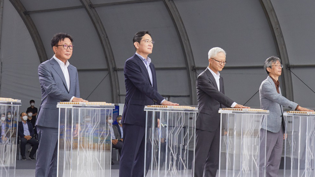
    Samsung Electronics today broke ground for a new semiconductor research and development complex in Giheung, Korea, aiming to extend its leadership in state-of-the-art semiconductor technology.

    Samsung Electronics plans to invest about KRW 20 trillion by 2028 for the complex in an area covering about 109,000 square meters within its Giheung campus. The new facility will lead advanced research on next-generation devices and processes for memory and system semiconductors, as well as development of innovative new technologies based on a long-term roadmap.

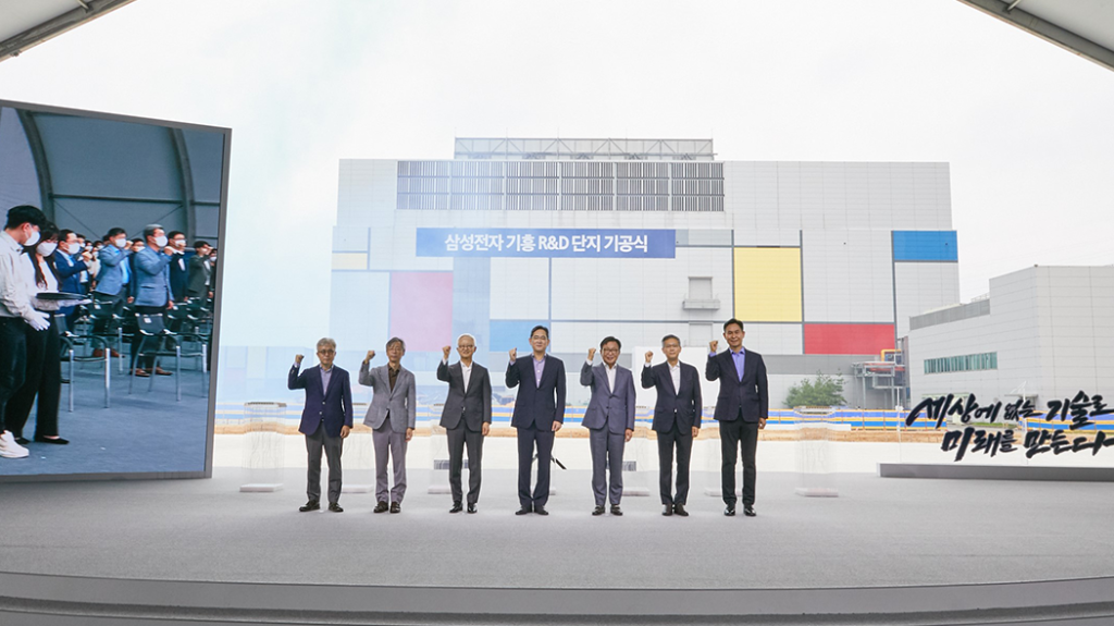
    Today’s groundbreaking ceremony was attended by Samsung Electronics Vice Chairman Jay Y. Lee, President and CEO Kye Hyun Kyung, President of the Memory Business Jung-Bae Lee, President of the Foundry Business Siyoung Choi and President of the S.LSI Business Yong-In Park, along with more than 100 employees.

    Mr. Kye Hyun Kyung, Device Solution President & CEO, SAMSUNG ELECTRONICS

    “Our new state-of-the-art R&D complex will become a hub for innovation where the best research talent from around the world can come and grow together,” said President Kye Hyun Kyung, who also heads the Device Solutions (DS) Division. “We expect this new beginning will lay the foundation for sustainable growth of our semiconductor business.”

    With the establishment of the new R&D facility, Samsung Electronics is seeking to overcome the limits of semiconductor scaling and solidify its competitive edge in semiconductor technology.

    Samsung Electronics’ Giheung campus, located south of Seoul near the DS Division’s Hwaseong campus, is the birthplace of the world’s first 64Mb DRAM in 1992, marking the beginning of the company’s semiconductor leadership.

    The new Giheung R&D facility, together with the R&D line in Hwaseong and the world’s largest semiconductor production complex in Pyeongtaek, is also expected to elevate the synergy among Samsung’s three main semiconductor complexes in the metropolitan area.

    After the ceremony, Vice Chairman Jay Y. Lee visited the Hwaseong campus to meet with employees of the DS Division, where they discussed ways to promote innovation within the company. At a separate meeting with executives of the DS Division, discussions involved current issues in the global semiconductor industry, progress of next-generation semiconductor technology R&D and ways to secure technology to expand semiconductor leadership.


    If you have an interesting Article / Report/case study to share, please get in touch with us at editors@roymediative.com/ roy@roymediative.com, 9811346846/9625243429.

    Breaks Ground extend its leadership Giheung Korea New Semiconductor R&D Complex Samsung Electronics semiconductor technology
    Share. Facebook Twitter Pinterest LinkedIn WhatsApp Reddit Tumblr Email
    MOBILITY INDIA

    Related Posts

    Tide turning in Europe’s smartphone market despite 6% shipment decline in Q3

    November 29, 2023

    Blaupunkt Redefines Sound Excellence with BE100 XTREME Neckband

    November 28, 2023

    Sony India unveils INZONE H5 wireless gaming headset to elevate your gameplay experience, advised by Fnatic

    November 28, 2023

    Comments are closed.

    YXL
    Top Stories
    Cover Story

    Nifty Gadgets You can Gift Your Loved Ones this Festive Season

    By MOBILITY INDIAOctober 18, 20230

    Follow @mobilitymag With festive season round the corner, the younger ones and also the mature…

    Cover Story

    TWS Market – Affordability & Appealing Aesthetics attribute to unparalleled performance

    By MOBILITY INDIASeptember 21, 20230

    Follow @mobilitymag Convenient and hassle-free way to listen to music TWS stands for True Wireless…

    Cover Story

    Sleek & Stylish Chargers to Energize Your Devices in No Time – Instant Fast Chargers that can fuel the devices

    By MOBILITY INDIASeptember 1, 20230

    Follow @mobilitymag A mobile charger is a portable charger that allows users to restore power…

    News

    Best Mobile Phones below 30K

    By MOBILITY INDIAJuly 5, 20230

    There are too many options available to the consumers when it comes to mobiles under…

    News

    First Made-In-India Chip To Be Rolled Out By December 2024: Minister

    By MOBILITY INDIAJune 27, 20230

    First Made-in-India chips are expected to be rolled out by December 2024, Union Minister for…

    About US
    Mobility-logo

    A-23, 1st Floor Okhla Industrial Area, Phase-1, New Delhi-110020 (India)

    Telephone: 011-41602841, 011-40536384 -87

    Mob No. : 09811346846, 09625243429, 08287406709

    Regd.Off.: 38-B/56 Block, C. R. Park, New Delhi-110019.

    My Story

    Retail jobs in India down 12 percent amid record festive sales

    By MOBILITY INDIAOctober 8, 20220

    Femina Miss India world, Ms. Sini Shetty visited U&i booth at Big 7 Expo

    By MOBILITY INDIAAugust 30, 20220
    1 2 3 Next

    Mobility Magazine November 2023

    By MOBILITY INDIANovember 11, 20230

    Make In India Mobility Magazine November 2023

    By MOBILITY INDIANovember 11, 20230

    Make In India Mobility Magazine October 2023

    By MOBILITY INDIAOctober 17, 20230

    Mobility Magazine October 2023

    By MOBILITY INDIAOctober 17, 20230
    Facebook Twitter Instagram LinkedIn YouTube
    • Home
    • Contact
    • About Us
    © 2023 Mobility India. Designed by Roy Mediative.

    Type above and press Enter to search. Press Esc to cancel.