

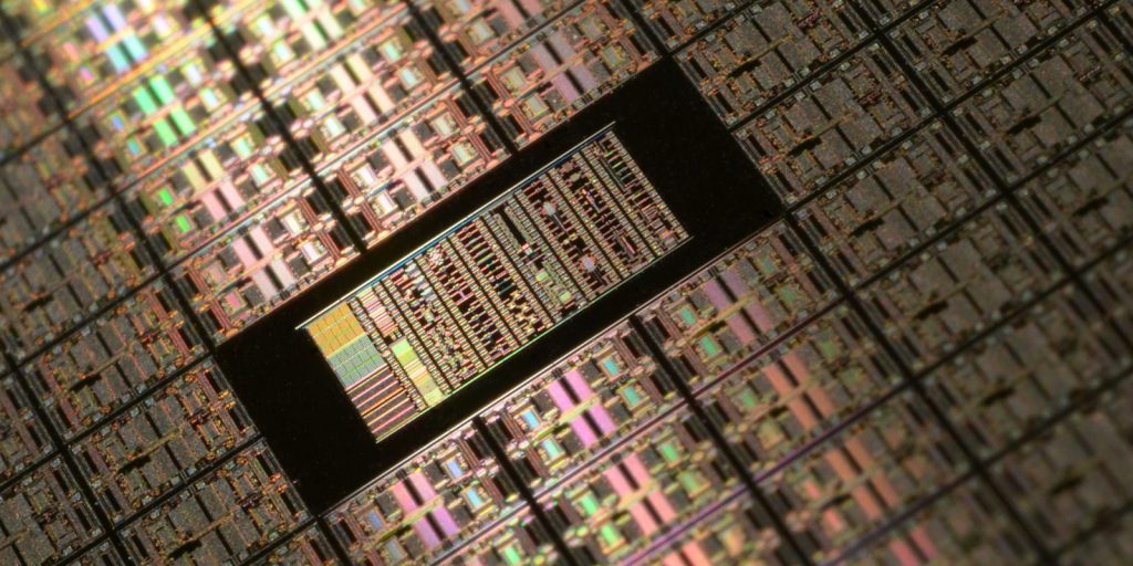
3mn chip fabrication is nothing but a new, improved generation of silicon semiconductor chips in terms of increased transistor density (i.e., a higher degree of miniaturization), increased speed and reduced power consumption.

The third generation of semiconductor materials has a wide bandgap, high breakdown electric field, high thermal conductivity, high electron saturation rate and higher radiation resistance.It is widely used in new energy vehicles, rail transit, smart grid, new generation mobile communication, consumer electronics and other fields, and is regarded as the core technology supporting the development of energy, transportation, information, defense and other industries. Many companies are opting for improved generation of silicon semiconductors. generation of silicon semiconductors.
Samsung Foundry, the South Korean chaebol’s semiconductor chip manufacturing arm, showcased that 5LPP and 4LPP processes will be used to mass-produce chips in high volumes 2021 and 2022, respectively. The company’s 3nm GAA (Gate-All-Around) technology is absent from the product roadmap.
TSMC is on track to move 3nm process technology (N3) to volume production in the second half of 2022 as scheduled, and will continue to see its 5nm process capacity fully utilized next year, according to industry sources.
The world’s largest contract manufacturer for chips Taiwan Semiconductor Manufacturing Company (TSMC), is reportedly set to being the production of chips based on a 3nm process next year.
According to DigiTimes, the company is not just planning for 3nm chips but will also have an enhanced version of the same in the form of N3E, which will go into production in 2023. High Volume Manufacturing (HVM) of the 3nm process node (N3) will start in the second half of next year.
N3E will feature improved manufacturing process window with better performance, power and yield.Compared with the 5nm process, the 3nm gate-all-around (GAA) node boosts performance by 30 per cent, lowers power consumption 50 per cent and takes up 35 per cent less space.In addition, TSMC and the Sony Group are reportedly considering joint construction of a semiconductor factory in western Japan amid a global chip shortage. The total investment in the project is estimated at 800 billion yen ($7 billion), with the Japanese government expected to provide up to half the amount.
In December 2019, Intel announced plans for 3 nm production in 2025. In January 2020, Samsung announced the production of the world’s first 3 nm GAAFET process prototype, and said that it is targeting mass production in 2021. TSMC plans risk production in 2021 with volume production in the second half of 2022.
Thus we see how companies have incorporated 3mn chip fabrication for improved generation of silicon semiconductor chips.